Introduction: Why Purity Matters in Semiconductor Applications
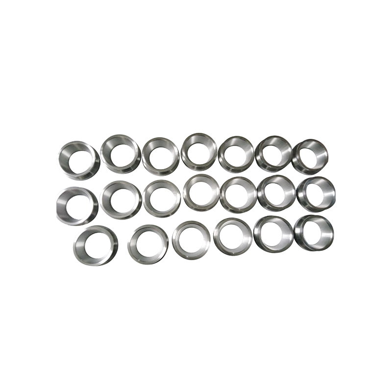
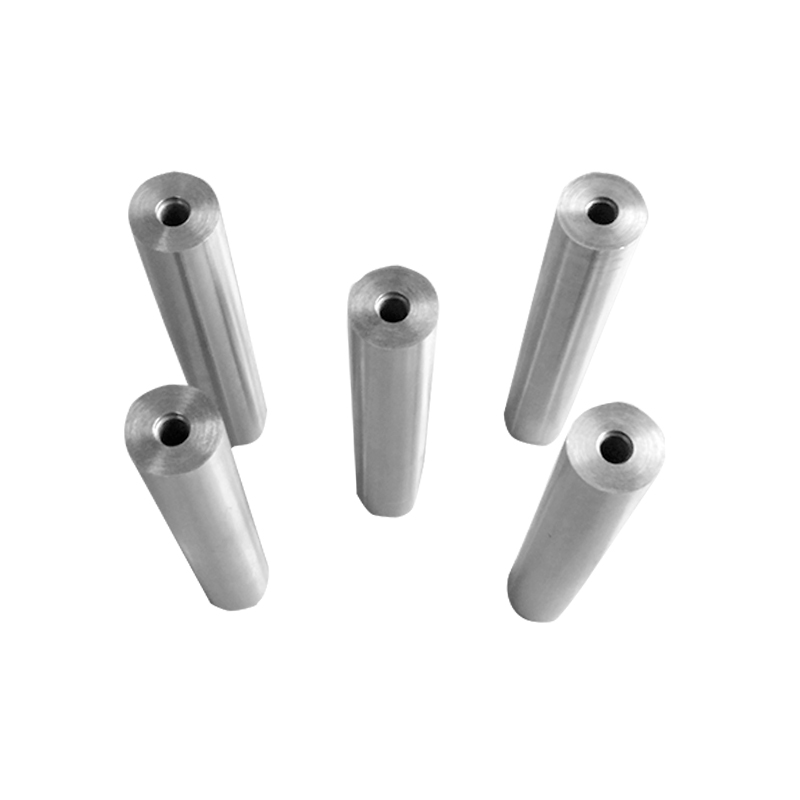
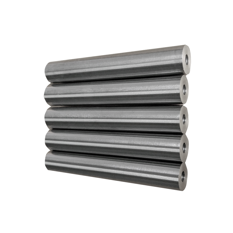
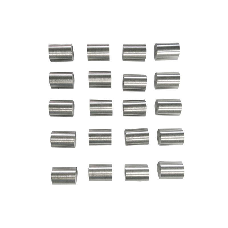
Molybdenum is a refractory metal widely used in semiconductor manufacturing — for heater elements, support rods, evaporation sources, sputtering targets, and wafer handling fixtures. In these roles, even trace impurities or entrapped gases can alter electrical behavior, contaminate vacuum processes, change evaporation chemistry, or accelerate localized corrosion. Therefore, specifying the correct molybdenum purity is the first step toward ensuring process stability and device yield.
Typical Purity Grades and Which Applications They Serve
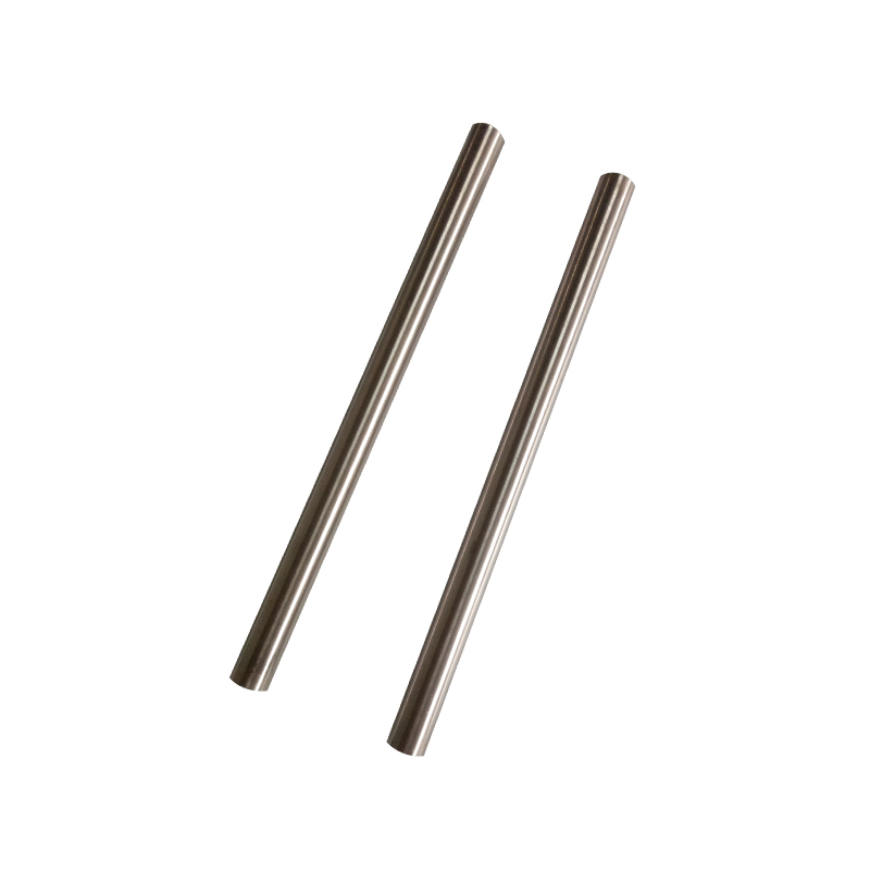
Molybdenum rod purities commercially range from industrial grades (≈99.0–99.8%) up to ultra-high purity materials (≥99.999%). For semiconductor use, purchasers most commonly select between high-purity (≥99.95%, often labeled 3N5) and ultra-high-purity (≥99.99% to 99.999%, labeled 4N–5N) depending on the component's proximity to active process zones and its role in vacuum deposition or contamination-sensitive steps. High-purity molybdenum (≈99.95%) is typical for structural components and heating elements; ultra-high purity (99.99%+) is preferred for evaporation/sputtering sources and any part that directly contributes material or surface species to a wafer process.
Which Impurities Matter (and Why)
Not all contaminants are equally harmful. Oxygen, carbon, nitrogen and sulfur can form brittle phases or change mechanical properties at elevated temperatures; iron, nickel, chromium and silicon can introduce undesired metallic contamination that diffuses onto wafer surfaces during high-temperature processing. For deposition sources, volatile impurities or inclusions can vaporize or sputter and deposit on device layers, causing defects or altered electrical properties. Therefore specs commonly limit these elements to single-digit ppm (parts per million) for the cleanest grades.
Common Specification Items in Purchase Documents
A clear specification reduces risk. Typical procurement specs for semiconductor-grade molybdenum rods include: declared overall chemical purity (e.g., ≥99.95%, ≥99.99%), maximum ppm limits for critical impurities (O, C, N, S, Fe, Si), density and porosity targets, acceptable mechanical properties (yield/UTS where relevant), surface finish, dimensional tolerances, and acceptable inclusion size/distribution. Suppliers for semiconductor markets often provide trace element analyses and certification reports with each lot.
Practical Table: Purity Grades vs. Typical Semiconductor Uses
The following table summarizes practical grade-to-application guidance used by fabricators and fabs when deciding what to buy.
| Purity Grade | Typical Impurity Limits | Recommended Semiconductor Uses |
| ≥99.90% (3N) | Impurities tens–hundreds ppm | Structural supports, non-critical fixtures |
| ≥99.95% (3N5) | Critical impurities single–low double-digit ppm | Heaters, chamber parts near but not in line-of-sight, some fixtures |
| ≥99.99% (4N) | Impurities typically <10 ppm for many elements | Evaporation/sputtering sources, crucibles, wafer-contact parts |
| ≥99.999% (5N) | Sub-ppm to single-digit ppm control for most species | Highest-sensitivity deposition, advanced R&D and ultra-clean processes |
How Purity Is Measured and Certified
Buyers should require laboratory certification. Common analytical methods include glow discharge mass spectrometry (GDMS) for multi-element trace analysis, inductively coupled plasma mass spectrometry (ICP-MS) after dissolution for soluble impurity profiling, and LECO combustion analyzers for precise oxygen/carbon/nitrogen quantification. For physical quality, density testing, metallography and porosity checks are standard. Reputable suppliers include certificates of analysis (CoA) and, if needed, batch-specific GDMS reports for ppm-level traceability.
Handling, Storage and Pre-Use Preparation to Avoid Contamination
Ultra-high-purity molybdenum requires care after delivery. Store rods in dry, clean packaging to prevent surface oxidation and avoid cross-contamination with lower-grade metals. During machining, use dedicated tooling and coolant strategies that do not introduce oils or tramp elements; where possible, perform final cleaning under clean-room-compatible solvents or in vacuum-bake cycles before installing parts into process chambers. For deposition sources, pre-bake and vacuum outgassing reduce trapped gases that might degas during high-temperature runs.
Procurement Best Practices and QA Clauses
When writing purchase orders for semiconductor applications include: minimum chemical purity, explicit ppm limits for critical elements, required test methods (GDMS/ICP-MS) and acceptance criteria, lot traceability, surface finish tolerances, and a clause for independent lab verification on arrival. Negotiate return or rejection terms tied to CoA discrepancies and maintain a qualified supplier list that can demonstrate historical consistency and traceable processing routes (e.g., powder source, sintering, swaging or vacuum arc-casting steps).
Cost vs. Purity Trade-Offs: Practical Recommendations
Higher purity costs rise steeply as you move from 99.95% to 99.999% due to tighter raw material control and more demanding processing and testing. Match purity to risk: use ultra-high-purity rods only where the component is likely to be a direct contamination source (e.g., evaporation crucible or target). For secondary supports and chamber fixtures, a well-characterized 99.95% material often provides a good balance of performance and price. Always quantify the potential yield or process risk avoided by moving to a higher grade before paying the premium.
Case Study: Choosing Rod Purity for an Evaporation Source
A fab replacing an evaporation boat must consider line-of-sight contamination and the vapor chemistry. If the molybdenum is used as an inert structural holder (no intended contribution to the film), 99.99% with sub-10 ppm critical impurities is commonly specified. If the molybdenum itself is the source material or is in intimate contact with evaporants, specifying 99.999% and requesting batch GDMS reduces risk of trace-metal inclusions in films. Run a small qualification evaporation and analyze deposited films for unexpected metallics before full deployment.
Conclusion: Specify, Verify, and Handle Carefully
For semiconductor manufacturing the required molybdenum purity depends on where the rod sits in the process chain. Use 99.95% (or 3N5) grades for non-line-of-sight structural parts and heaters, 99.99% (4N) for components close to wafers and for many deposition roles, and reserve 99.999% (5N) for the most contamination-sensitive, R&D or advanced-node deposition tasks. Whatever the grade, insist on documented analysis (GDMS/ICP-MS), clear ppm limits for critical species, and clean handling procedures to preserve the material’s integrity from receipt to installation.
Quick Checklist for Engineers and Buyers
- Define the component’s proximity to active wafer processes (line-of-sight vs. structural).
- Specify a minimum purity and list ppm maximums for O, C, N, S, Fe, Si and other critical metals.
- Require GDMS or ICP-MS CoA and hold a right-to-audit/independent test clause in the PO.
- Plan handling: clean-room transfer, dedicated tooling, pre-bake/vacuum conditioning where applicable.
- Balance cost vs. contamination risk—only pay premium for purity where failure or yield loss justifies it.


